Project Info
The HP-DDR3 Controller is a high-performance, special-purpose memory controller that interfaces with industry standard DDR3 SDRAM memory devices and provides a common command interface for the user applications.
Description
This core is aimed at optimizing both performance and resource usage: it is designed focusing on the logic level reduction. The controller adapts the execution of memory access commands in order to exactly match the timing requirements imposed by DDR3 device parameters. The memory controller supports burst memory read and write accesses with dynamic burst size. It also manages memory initialization and refresh cycles autonomously. The core is fully configurable through VHDL generics. In the IP core a Multiport Controller module is included to support the contemporary access from several modules to the DDR3 device.
| IP core Specifications | |
|---|---|
| Supported FPGA Family | Lattice ECP5* |
| HDL format | VHDL/EDIF |
| Verification support | Test-bench |
| Tool requirements | Diamond 3.7 or higher |
* speed grade -8 is required to reach DDR3-800 standard due to the specific Lattice technology timing characteristics
Key Features
- High Performance DDR3-800
- Interfaces to industry standard DDR3 SDRAM devices and modules
- Low FPGA resource utilization
- Supports unbuffered DIMM
- Various SDRAM data path widths support
- Variable address SDRAM width
- Configurable CAS latency
- Configurable memory timing parameters
- Command burst capability with dynamic burst size control
- Byte-level writing through data mask signals
- Automatic auto-refresh
- Multiport Controller
- Wishbone Bus Interface (optional module)
Architecture
The finite state machine controller is a very compact and carefully optimized implementation that permits the achievement of high operational frequencies. Nevertheless, it manages DDR3 memory initialization and auto-refresh. For each user command the sequence of DDR3 commands consisting of active, read/write, and precharge is performed by the controller. The core has been optimized to execute the above commands sequence in the minimum time, excluding bank management (i.e. simultaneously active rows in different banks) from the implementation. This permits to achieve the minimum latency for accesses spread across the whole memory, typical of multiport applications. Moreover it makes the real performance evaluation independent from the user application since each command is executed in a constant time.
Resource usage and Performance
The resource usage has been evaluated adopting Diamond 3.10 tool on a LFE5UM-85-8 device. Needed SLICES, LUTs and registers are listed in the table (values are rounded). The maximum I/O frequency reachable in the Lattice ECP5 family (higher speed grade) is guaranteed, while the internal core logic works at 200MHz.
| Resource Utilization (Lattice ECP5) | ||||
|---|---|---|---|---|
| Data Bus Width = 16 (Burst=8) | ||||
| SLICEs | LUTs | Registers | f Max | f Sysclk |
| ~1000 | ~900 | ~1300 | 400MHz (800Mbps) | 200MHz |
| Data Bus Width = 32(Burst=8) | ||||
| SLICEs | LUTs | Registers | f Max | f Sysclk |
| ~1300 | ~1000 | ~1900 | 400MHz (800Mbps | 200MHz |
Core version
The current IP core version is 1.0.
Verification
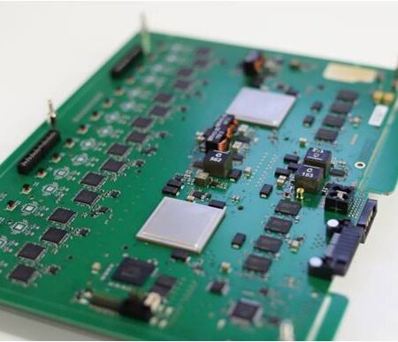
The IP core has been implemented with Diamond 3.10 design tool. It has been tested on a custom board mounting MT41K128M16JT DDR3 device.
Optional modules
The Wishbone Bus Interface can be provided as optional VHDL module.
Sanitas EG reserves the right to change specifications without notice


